|
LAB 03. Morphological and Structural Characterizations
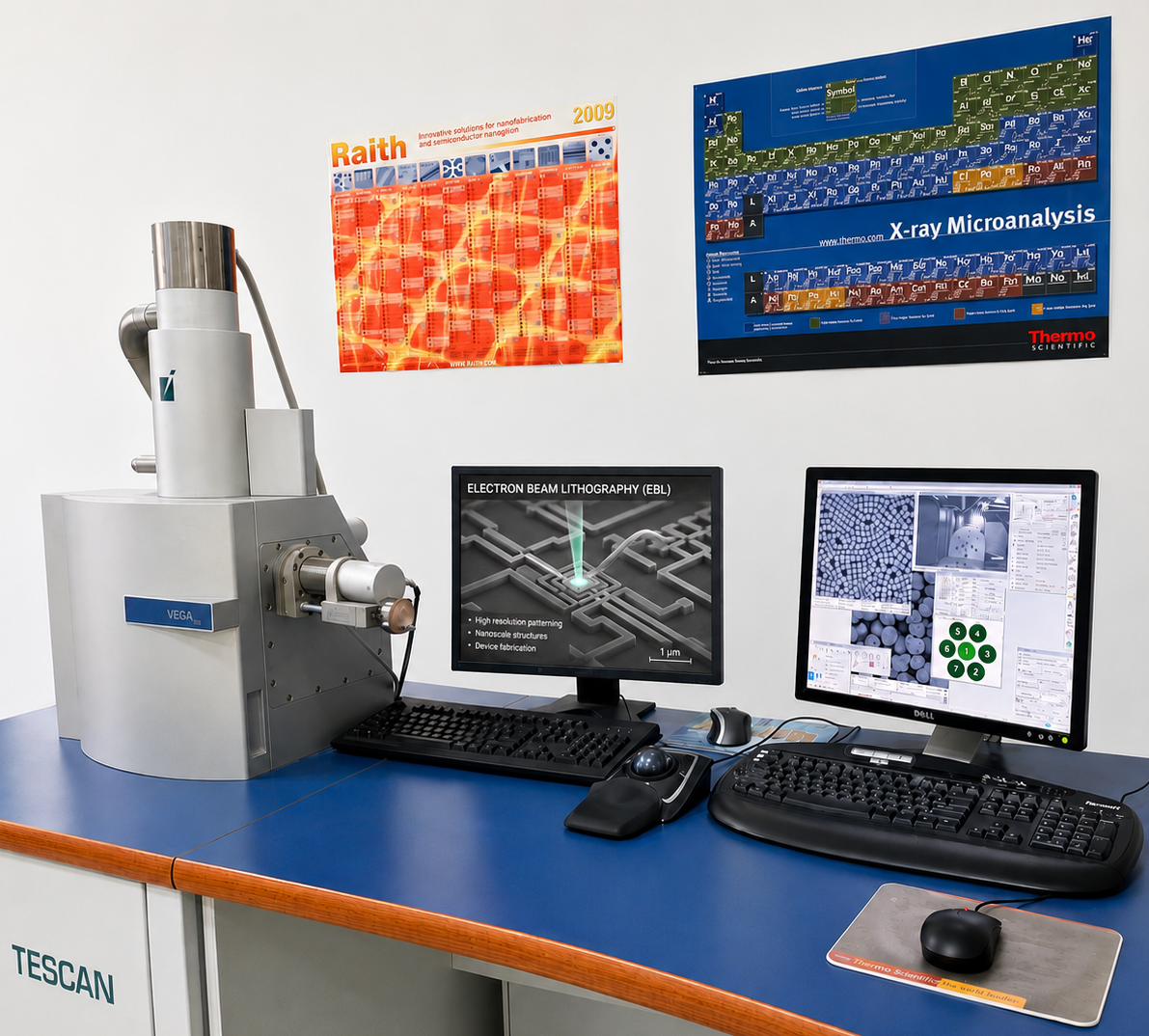
Scanning Electron Microscope (SEM)
TESCAN Vega XM, Czech Republic
Specifications:
- Thermionic emission filament
- Five axes fully monitorized stage
- Secondary electron detector (SED)
- Backscattered electron detector (BSED)
- Medium and high vacuum operation
- Electron beam lithography (EBL), RAITH module
Applications:
- Surface and interface morphology studies
- Cross-sectional analysis of samples
- Electron beam nanolithography (EBL)
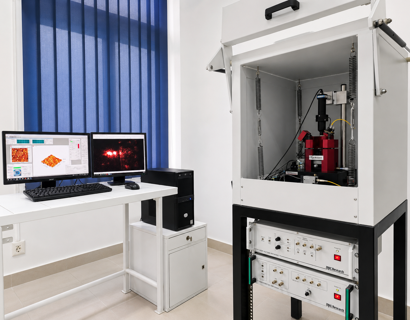
Atomic Force Microscope (AFM)
A.P.E.Research A100-SGS, Italy
Specifications:
- AFM, "contact" and "tapping" mode
- Conductive-AFM (C-AFM)
- Electrostatic force microscopy (EFM)
- Magnetic force microscopy (MFM)
- Piezoelectric force microscopy (PFM)
- Scanning tunneling microscopy (STM),
environmental
- Nanolithography module:
- Nano-indentation ("Scratching")
- Local anodic oxidation (LAO), equipped with a relative humidity (RH) regulation and control system
Applications:
- Surface morphology and topography studies, including the extraction of quantitative parameters (RMS roughness, skewness, kurtosis, etc.)
- Local probing of electrical, magnetic and piezoelectric properties of nanomaterials
- Fabrication of nanostructures and functional patterns by high-resolution nanolithography
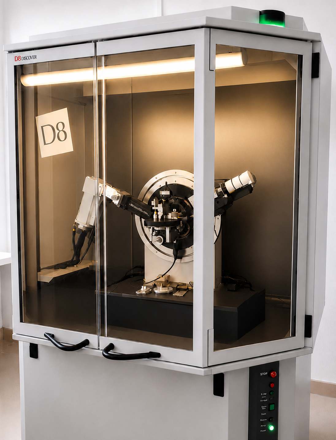
X-ray Diffractometer (XRD)
Bruker D8 Discover, Germany
Specifications:
- X-ray radiation: Copper (Cu) Kα1 și Kα2
- Optimized for the analysis of crystalline powders (PXRD)
- Grazing-incidence X-ray diffraction (GI-XRD) capability
- X-ray reflectometry (XRR) module
Applications:
- Identification of crystal systems and crystalline phases
- Advanced structural analysis with the determination of crystallographic and microstructural parameters, including crystallite size (coherence length), microstrain, lattice parameters and degree of crystallinity
- Evaluation of thin-film and multilayer morphological parameters by X-ray reflectometry (XRR)
Accessories, consumables and auxiliary tools available in the lab:
- Tweezers available in a wide range of shapes, sizes, and functional configurations, manufactured from stainless steel, Teflon, and other materials compatible with laboratory applications. They are used for the handling, positioning, and transfer of samples and sensitive specimens during experimental procedures.
- Comprehensive set of accessories for high-resolution microscopy, including dedicated sample holders and specimen stubs for various types of samples, mounting and fixation systems, conductive carbon adhesive tapes used for sample preparation and mounting in electron microscopy applications, as well as other consumables and auxiliary components required for the morphological and structural characterization of advanced materials.
- Access to crystallographic databases (PDF, COD, ICSD, etc.) for identification and validation of crystalline phases through correlation of experimental diffraction patterns with reference data and crystal structures reported in scientific literature.
- Laboratory gloves, lab coats, safety goggles and other personal protective equipment.
|
 Research & Development Center for Materials and Electronic & Optoelectronic Devices
 Faculty of Physics
 University of Bucharest
Video presentation
Visit the old site
|
©MDEO, Faculty of Physics, University of Bucharest
|
|